グラフェン
| | References and the source which I can inspect are not shown at all, or this article is insufficient. You add the source, and please cooperate with the reliability improvement of the article. (July, 2015) |
With グラフェン (graphene), it is the seat of the sp2-binding carbon atom of the thickness of 1 atom. I take the hexagonal lattice structure such as the made hive out of a carbon atom and the combination. The origin of the name from graphite (Graphite) and "ENE." A lot of グラフェンシート pile up and have graphite in itself, too.
Bond distance between carbon of グラフェン is approximately 0.142nm. It is the basic structure of the carbon allotrope (graphite, carbon nanotube, fullerene).
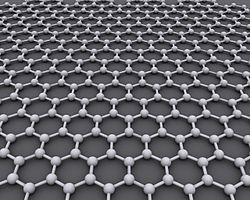
Table of contents
Explanation
Combination between carbon is stronger than a diamond and is thought with the material which is stronger than a diamond in the plane. It is very strong physically and is the strongest in pulling in the world. It is said that the heat conduction is the best in the world, and the electric conduction degree is the material which is good in the top-class, too.
In complete グラフェン, the cell of a pentagon and the heptagon becomes the lattice defect only from the set of the hexagonal cell. When a five-cornered cell stands alone and exists, as for the plane, the thing that the cell of the heptagon stood alone in the same way which is sharp into a corn form (12 five-cornered cells form fullerene) bends a seat to a saddle type. I can bring about various shapes such as the carbon nano bad by controlling the introduction of a pentagon and the heptagon cell. I can consider the carbon nanotube consisting of one level to be グラフェン of the barrel (a hemisphere chief of グラフェン consisting of six five-cornered cells may hold the end). Andre ガイム (Andre Geim) and Constantine ノボセロフ (Konstantin Novoselov) won Nobel Prize in Physics by a pioneer experiment about two-dimensional material グラフェン in 2010 [1].
Manufacturing method
It was difficult to obtain グラフェン until it was the 2000s, and the study of this field did not advance for many years. Because グラフェン came to be got by sticking a fragment of the graphite (black lead) on cellophane tape (scotch tape) in 2004, and tearing it off, an applied study of グラフェン advanced [1].
With "CVD" (CVD) to supply gas containing carbon to the board which formed technique and a catalyst metal layer pyrolizing silicon carbide (SiC) "the scotch tape method" to get グラフェン by tearing it off with the adhesive strength of the cellophane tape because グラフェン is tied by weak van der Waals forces of the cohesion in the thing which グラフェン-formed as for two dimensions of graphite plurally laminated up and down, and form lamellar structure [1].
Characteristic
Conductive
From a laboratory finding, the electronic mobility in グラフェン is surprisingly high at room temperature with 15,000 cm2V-1s-1. In addition, I understand that an electric conductivity is symmetric from an experiment, and this suggests that an electron and the mobility of the hall are about the same. Because I hardly depend on the temperature in the range of 100 K, mobility is thought of by 10 K that a lattice defect is a main cause of the dispersion. For dispersion by phonon in グラフェン, the mobility at the room temperature is limited in 200,000 cm2V-1s-1 (carrier density at the time of 10-12cm-2), but the resistance corresponding to this is 10-6 Ω, cm. This value is the resistance level that is smaller than silver which is the material that resistance at the room temperature is the smallest. However, influence of the electronic dispersion by the optics phonon of the board is bigger than dispersion by the phonon of グラフェン oneself, and, in グラフェン on the silicon dioxide board, the mobility is limited at room temperature to 40,000 cm2V-1s-1.
Though carrier density is zero in the D rack point neighborhood; グラフェン I show the smallest electric conductivity of the の order. I do not yet become clear in the origin of this smallest electric conductivity. However, I tear off グラフェンシート and I can localize the puddle of the carrier by mixing the impurities which ionized with SiO2 board and come to conduct it. A conduction degree smallest as for some theories The estimate that I explain it, but であることを is often found I depend on the density of impurities after being order more than かそれ.


It has been proved that chemical dopant affects the mobility of carriers in グラフェン by a recent experiment. The Schedin and others doped a various gas class (a certain thing becomes the acceptor, and a certain thing is a donor) in グラフェン and found that グラフェン structure before the dope reappeared by heating グラフェン slowly in vacuo. When dopant density is beyond 1012cm-2, the Schedin and others report it to the mobility of the carrier when there was not the conspicuous change. The Chen and others dope potassium at an ultrahigh vacuum, low temperature in グラフェン and an expected potassium ion behaves as electric charge impurities in グラフェン and finds that 20-fold decreases mobility. I can return the mobility that decreased by heating グラフェン, and removing potassium.
Optics properties
While グラフェン is 1 laminar structure of the carbon atom by the unique electrical characteristic, opacity is unexpectedly high. The absorption factor of the sunshine of グラフェン is the surprisingly simple price of π α ≒ 2.3%. α is the microstructure fixed number here. This is a fact checked experimentally, but is not the measurement that is correct so as to be usable for the improvement of the value of the microstructure fixed number.
Spin transportation
Because spin orbit interaction is small, and a nuclear magnetism moment of carbon can ignore グラフェン again, it is thought with ideal materials of the spintronics. Introduction, the detection of the electrical spin style at the room temperature was shown recently. The spin coherence length more than 1 micrometer is observed at room temperature and can control the direction of the spin style with an electrical gate at the low temperature.
Magnetic field effect
In addition to high mobility and the smallest electric conductivity, グラフェン behaves in a very interesting way in a magnetic field. With the quantum Hall effect normal in グラフェン a system The abnormality quantum Hall effect that hold it, and slipped off is caused. In other words, the hall conductivity である. Here In the index of は Landau levels by the double degeneration of two valleys and spins の factor occurs. This characteristic behavior can be observed at the room temperature. Double layer グラフェン shows quantum Hall effect, but it is normal quantum Hall effect to take place in double layer グラフェン, である. It is the first plateau Because は does not exist, it is suggested that double layer グラフェン becomes metallic at a neutral point.


A phase gap only for π known as berry phase is seen in グラフェン. Because the effective mass of the carrier becomes zero as for berry phase in a D rack point neighborhood, I produce it. From a temperature-dependent study of Shubnikov-de Haas vibration in グラフェン, I knew that the carrier which behaved as effective mass zero had limited cyclotron mass by energy - cycle dispersion relations.
擬相対論
The electrical characteristic of グラフェン is explained in a traditional tight binding model. It is a cycle in this model I can write the energy of the の electron as follows.


Here Energy, the grating constant that a hop does in は 最近接原子 . A dispersion-related plus and the negative mark support a conduction band and valence band each. The valence band contacts with a conduction band with six points called K-values, but it is only two points to be independent in six points, and remaining is equivalent from symmetricalness. The energy becomes linear, but it is similar to the dispersion relations of the particle of the relativism in this in a cycle the near K-point. Furthermore, the wave function lasts to 2 spinor structure effectively because the unit cells of the lattice consist of 2 atoms. As a result, D can write the electron by a rack equation and an equation equivalent formally by low energy. A limit chiral as for the description that is this 擬相対論的 namely rest mass But, interesting various characteristics occur because I am limited by a limit of zero.


Here It is fermi speed of は グラフェン and takes place of the velocity of light of the D rack theory. It is the vector of the は Pauli line, It is a wave function for the hermaphrodite of the は electron. It is は energy. Briefly, the electron in the top of デラックコーン is in a condition to disagree with an uncertainty principle of Heisenberg decided at a position and the point with the momentum. However, you are going to evade the reciprocity of the uncertainty principle by increasing position width and momentum breadth by a relativism effect and should think that therefore electronic speed suddenly grows big.


Use
The uses such as semiconductor element and transparence conductive films such as the field effect transistor are thought about [1]. The development of the spaceship which advances by irradiating a microwave like sun sail is studied [2].
Commercial production
As for the technique to enable the グラフェン production on the commercial scale, the team of the Polish ヴウォジミェシュ ストゥルピンスキ doctor (Dr. Wlodzimierz Strupinski) succeeded in development in 2011.
I begin full-scale production now in Polish nano carbon company.
Footnote
Allied item
- Carbon
- Graphite
- A generic name of グラフェン with size of the ナノグラフェン - nano scale size.
- Quantum Hall effect
- Nobel Prize in Physics
- Andre ガイム
- Constantine ノボセロフ
- Rag fen
Outside link
This article is taken from the Japanese Wikipedia グラフェン
This article is distributed by cc-by-sa or GFDL license in accordance with the provisions of Wikipedia.
In addition, Tranpedia is simply not responsible for any show is only by translating the writings of foreign licenses that are compatible with CC-BY-SA license information.
0 개의 댓글:
댓글 쓰기